

All electronic devices eventually die, and the failure can be quite spectacular if suitable foresight and care was not employed during the design and construction phases, especially if the device handles high power or is supplied by a large battery. It should go without saying that both conditions apply to much of the electronics inside an EV, so a closer look at where and how power electronics fail and how to minimize the collateral damage will be the focus of this article.
Although there are myriad precipitating or apparent causes of failure, the ultimate cause is usually thermal in nature; that is, overheating. The only real exception is failure due to overvoltage puncturing an insulator, such as the gate oxide layer in a MOSFET or IGBT. Applying too high a voltage across a reverse-biased or turned-off semiconductor (PN) junction will cause it to start conducting through a process called avalanche breakdown, but it might be surprising to learn that no harm will result as long as current is limited. This is how most Zener diodes work, actually (those with a breakdown voltage above 4 V or so), but aside from Zeners and a few specialized devices/circuits typically used to create short, sharp pulses, avalanche breakdown is an unwelcome – and unplanned-for – phenomenon. Consequently, if a switch or diode undergoes avalanche breakdown, it frequently fails a few nanoseconds later from extreme overcurrent.
The most common cause of avalanche breakdown in power electronics – besides overvoltage on the supply line – is from the spike produced during turn-off by any stray (or “unclamped”) inductance in between the switch and the input capacitor (or between each switch in an inverter leg). This spike is produced because inductors resist any change in the flow of current through them, and while the inductances involved here are (or should be!) very small – on the order of a few tens of nanohenries at most – the currents can be quite high and the switching times quite short.
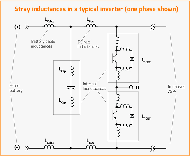
The actual equation that describes the voltage produced by an inductor experiencing a change in current is V = L * (dI / dt), where V is in volts, L is in nH and dI / dt is the change in amps per nanosecond. Given that a single wire in free space has an inductance of about 8-10 nH per cm, and that the voltage spike will be 1 V for every 1 A / 1 ns per 1 nH of inductance, it’s apparent that serious attention must be paid to minimizing the stray inductance by bringing the forward and return conductors as close together as possible (which cancels out the magnetic fields – and therefore the inductance – from each) or else resort to more complex circuits to either recycle the energy stored (e.g. resonant operation or active clamps) or to dissipate it as heat in passive snubbers. While lengthening the turn-off time will reduce the magnitude of the spikes, it also increases the switching losses, and if taken too far will also result in device failure; a case in which the cure is worse than the disease. Finally, degradation of the input capacitor – that is, a loss of capacitance and/or an increase in its Equivalent Series Resistance (ESR) – can also cause the turn-off spikes to increase over time; this is a particular issue with electrolytic types, as they literally dry out with age or use.
Overcurrent is another proximate cause of failure, but unlike overvoltage, in which there is a clearly marked delineation between what is tolerable and what isn’t, current rating is a much more nebulous parameter. This is because the current rating of a semiconductor mainly depends on how effectively heat can be removed from it. Other effects such as the number of charge carriers available, thermal inertia, etc. affect the ultimate current permissible through a semiconductor device, but at timescales longer than a few minutes you can just about push as much current through it as you want so long as you keep it from getting too hot. The key parameter in the datasheet to check is the thermal resistance from the junction to either the case (you specify the heatsink) or the ambient (they specify the heatsink) and the maximum junction temperature allowed, which is usually 100° C (though it can be much higher for newer silicon carbide devices). Even reputable manufacturers can play fast and loose with all the specs involved here, so it definitely pays to run a few calculations as a sanity check before spec’ing a part.

For example, one 1,200 V / 600 A IGBT datasheet specifies a thermal resistance from junction to case of 0.049° C / W and a maximum voltage drop of 2.40 V at 100° C, so this device can theoretically handle 637 A as long as the case is kept at 25° C. To actually achieve the datasheet spec of 600 A while keeping the junction below 100° C at an ambient of 25° C, however, the total thermal resistance from junction to ambient cannot exceed 0.0521° C / W. Given that the IGBT already uses up 0.049° C / W of that in the junction to case, the heatsink can’t contribute any more than 0.0031° C / W of additional thermal resistance. While this isn’t technically impossible to achieve with an exposed-pipe liquid-cooled heat exchanger with sufficient coolant flow, it definitely qualifies as “heroic measures required” (especially since losses from switching haven’t been considered, much less operating at an ambient higher than 25° C). As a heatsink with such vanishingly small thermal resistance tends to cost a lot, while competitive market pressures steeply penalize designs that are too conservative, the best compromise is to monitor the temperature as close to the junction as possible – the aforementioned device includes a thermistor right next to one of the IGBT dice inside – and start derating the allowed current once temperature climbs above a certain point.
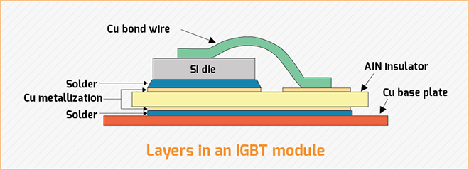
The other effects that come into play at even higher currents (and much shorter timescales) are bond wire vaporization (i.e. acting like a fuse), desaturation, current crowding and other safe operating area (SOA) violations. Bond wire vaporization is fairly self-explanatory: bond wires are the very small-diameter wires that interconnect the semiconductor die or dice to external terminals so they are very much like the fuses they so resemble (failure from repeated thermal cycling will be addressed below). Desaturation is a phenomenon in which the voltage drop across a switch that is otherwise supposed to be fully on starts rising sharply as if it were only partially on. While this term is most commonly applied to IGBTs (or other bipolar devices) because they exhibit the effect most strongly, it can occur in any semiconductor, and is the result of running out of charge carriers (“holes” in p-type material; electrons in n-type). Desaturation is especially pronounced in bipolar devices (like IGBTs) because voltage drop in them remains fairly constant over a wide range of current – usually in the range of 1.5 V to 2.5 V for modern IGBTs – but increases to 7 V or more at some level of overcurrent (usually >3x rated current). The voltage drop in unipolar (or “majority carrier”) devices such as MOSFETs is basically ohmic in nature until desaturation occurs, so it will likely already be quite high by the time the device truly enters desaturation (and it will have long since failed from overheating, too). The sharp rise in voltage drop during desaturation in IGBTs makes it a convenient proxy for detecting overcurrent and short-circuits in them (less so for MOSFETs), but the protection circuit needs to act fast, because a steep increase in voltage drop times an already excessive current means extraordinary amounts of heat are being generated in the junction. Consequently, even those IGBTs which claim to be “short-circuit tolerant” need to be turned off within 10 microseconds of entering desaturation (while those that don’t make such claims might survive such abuse for 1 µs at most).
Current crowding is basically desaturation that is localized to the area surrounding the gate contact(s), and it occurs to some extent every time an IGBT is in the process of turning on or off, due to the time it takes the change in operating state to propagate throughout the die (this effect is virtually non-existent in MOSFETs). Current crowding used to be a major problem in the older Bipolar Junction Transistor (BJT) technology that predates IGBTs, but the use of massively parallel and cellular construction – splitting one big switch up into many hundreds of smaller switches in parallel, basically – has nearly eliminated it.
A related problem is the SOA violation, which occurs when the product of the voltage drop across a device and the current through it exceed the safe operating area. When the switch is fully on, the voltage drop across it is very low, and while the switch is off the current through it is zero, so dissipation is low or zero, respectively. During the transition from each state, however, the voltage drop is high, while current might also be high – the device is acting more like a resistor than a switch. For example, a switch that is supplied by 300 V at a current of 100 A experiences a worst-case instantaneous power dissipation of 30 kW right before it fully turns off. When integrated out over the course of a full switching cycle the average dissipation loss from switching should be quite low, but that assumes that the transition time is a small fraction of the cycle time (a rule of thumb is to aim for transition time in the range of 0.5-1% of the period). This is why you don’t want to make the switching times any longer than necessary (nor increase switching frequency arbitrarily). The graph of allowable voltage drop vs current is called the safe operating area for the device, and while modern MOSFETs and IGBTs generally have “square” SOA curves – that is, can tolerate both maximum current and voltage at the same time – they also are infamously intolerant of operation in the linear region (i.e. like a resistor).
The last major cause of failure is thermal fatigue, which can affect the bond wires, semiconductor dice, the solder which attaches the dice to the heat spreader, the ceramic insulator used between the heat spreader and baseplate, etc. Thermal fatigue occurs when there are mismatches in the coefficients of thermal expansion of the various layers bonded together (die, substrate or heat spreader, insulator, baseplate, solder, etc) which are then subjected to temperature variations. The differences in the rate of expansion of each layer induces mechanical stresses proportional to the change in temperature. If the temperature swing is too wide and/or there are too many hot/cold cycles, then cracks in any of the layers, or voids in the solder, specifically, can develop. Thermal fatigue is the one failure mode guaranteed to strike down a power semiconductor if nothing else gets to it first. While there are simple solutions to this problem – such as the springs that Semikron uses to press the dice, heat spreader and insulator against the baseplate in their lower-power modules – they invariably suffer from a much higher thermal resistance and/or assembly cost. Consequently, this is one failure mode we all have to live with, but with good design and careful assembly the inverter, charger, etc, in an EV should outlast the batteries, motor and most of the moving parts.
This article appeared in Charged Issue 40 – November/December 2018 – Subscribe now.
Source: Electric Vehicles Magazine
